Thursday, October 31, 2019

EC8392 - Digital Electronics : Tutorial problems K-Map


EC8392 - Digital Electronics

Tutorial problems

Topic : K-Map

1. Simplify the Boolean expression of the function using K-Map & Implement using NAND gate

          i. F(a,b,c,d) = S(1,2,3,4,7,9,10,12)

         ii. Y(A,B,C,D) = S(1,4,6,7,8,10,11,15)

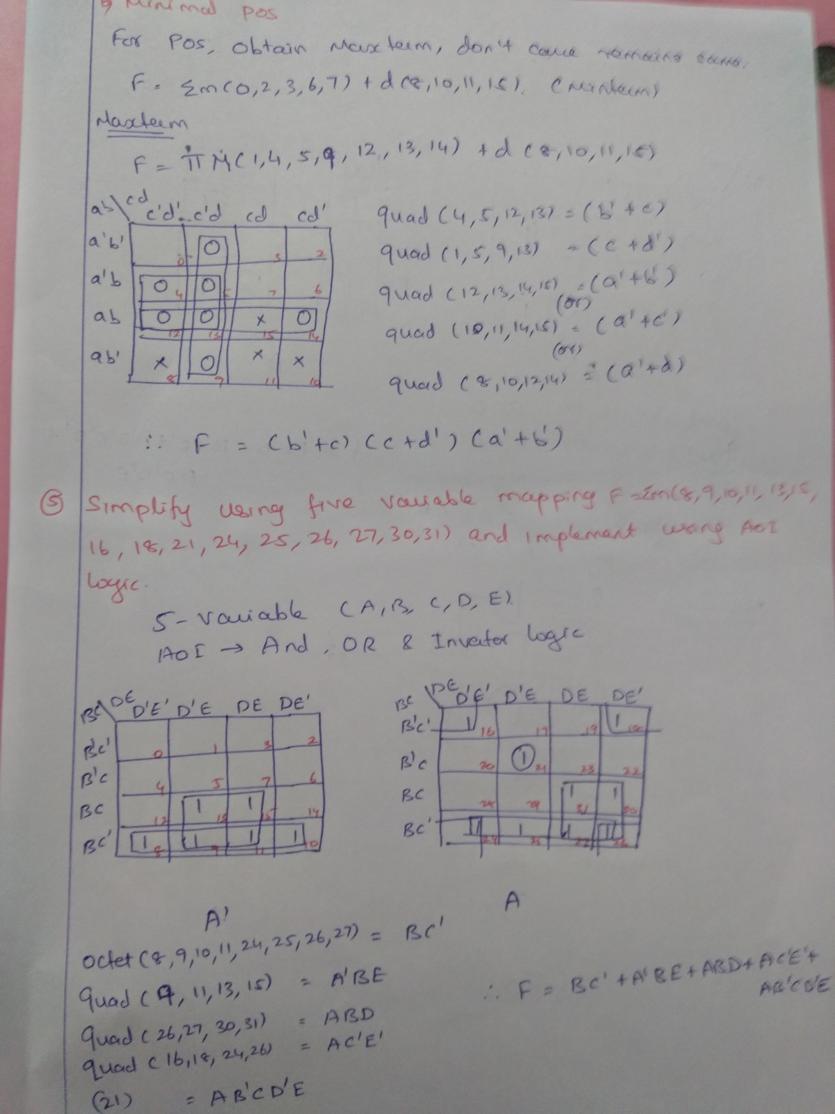
        iii. F = S(0,2,3,6,7)+d(8,10,11,15)

        iv. f(a,b,c,d) = S(1,2,3,9,12,13,14)+d(0,7,10,15)

        v. F=S(8,9,10,11,13,15,16,18,21,24,25,26,27,30,31)

        vi.F=S(1,4,6,10,20,22,24,26)+d(0,11,16,27)


2. Simplify the Boolean expression of the function using K-Map & Implement using NOR gate
        
        i. f(a,b,c,d) = P (1,2,3,4,7,9,10,12)

       ii. F(A,B,C,D) = P M(0,1,4,7,8,10,12,15)+d(2,6,11,13)

      iii. F = P M(4,6,8,10,12,15,16,18,19,20,22,23,25,27,29,30,31)+d(2,5,9,11,17,24)

Sunday, October 13, 2019

EC8392 - Digital Electronics Tutorial Sheet


8085 Microprocessor


1. The  Program counter in a 8085 microprocessor is a 16-bit register, because

Ans  : There are 16 address lines. 8085 has 16-bit address bus

2. In Intel 8085A microprocessor ALE signal is made high to

Ans : Enable the data bus to be used as low order address bus

ALE stands for Address Latch Enable. It is the 3oth pin of 8085 which is used to enable or disable the address bus. the address bus will be enabled during the 1st clock cycle as the ALE pin goes high i.,e logic '1' during the first half cycle

3. In 8085, which of the following modifies the program counter?

Ans : All instructions (PCHL, ADD, JMP & CALL)

4. If CS=A15’A14A13 is used as the chip select of a 4K RAM in an 8085 system, then its memory  range will be 

Ans: 6000H - 6FFFH and 7000H - 7FFFH 

5. The contents of a register (B) and Accumulator (A) of 8085 microprocessor are 49H and 3AH respectively. The contents of A and the status of carry flag (CY) and sign flag (S) after executing SUB B instruction are 

Ans : A=F1,  CY=1,   S=1


6. Which block within a microprocessor performs the integer arithmetic and bit-wise logical operations?

Ans : Arithmetic Logic Unit

7. An 8 Kbyte ROM with an active low chip select input CS is to be used in an 8085 microprocessor based system . The ROM should occupy the address range 1000H to 2FFFH. The address lines are designated as A15 to A0, where as A15 is the most significant address bit. One of the following logic expression will generate the correct CS signal for this ROM ?

Ans  : A15 + A14 + A13A12 + A13’A12  

8. The clock frequency of an 8085 microprocessor is 5 MHZ. If the time required to execute an instruction is 1.4µs, then the number of T-states needed for executing the instruction is 

Ans :  7

As Clock Frequency = 5 MHZ , time period (1/f) = 0.2µs, therefore for 0.2µs X 7 = 1.4µs

9. The following five instructions were executed on an 8085 microprocessor.
MVI A, 25H
MVI B, 91H
ADD B
CMA
ANI 68H
The accumulator value immediately after the execution of the fifth instruction is 

Ans : 48H


10. An 8085 assembly language program is given below. Assume that the carry flag is initially unset. The content of the accumulator after the execution of the program is
MVI A,07H
RLC
MOV B,A
RAL
RLC
ADD B
RRC

Ans : 23H


11. After the execution of the instruction XRA A the contents of A , carry and zero flags are respectively

Ans : A=00, CY=0, Z=1

As XRA is Exclusive OR operation, it will result as zero. The XRA A instruction is used to clear the contents of the Accumulator and store the value 00H.

12.  An RRC instruction in 8085 microprocessor instruction set will affect 

Ans : Carry Flag 

In 8085 Instruction set, RRC stands for “Rotate Right Accumulator”.  In this right rotation, the least significant bit will come out from the Accumulator and will be copied to CY bit in the flag register and also will be copied to the most significant bit position of the Accumulator.

13. What is the difference between MOV and MVI instructions of an 8085 microprocessor?

Ans : MOV instruction copies data between two registers, where as MVI instruction transfers an immediate data into a register.

14. In 8085 addition which of the following flags are set  when the addition of MSBs is more than 10?

Ans : Carry flag

15. The following instruction indicates which types of addressing mode?
LDAX B

Ans : Indirect address mode

LDAX stands for LoaD Accumulator indirect from register pair (X), and again by the name, you can tell that it uses indirect addressing.

BCD Adder / Decimal Adder


Click the below link for BCD Adder / Decimal Adder 's explaination

BCD Adder / Decimal Adder

Sunday, October 6, 2019

VHDL and Microprocesser Basics


1. Which of the following statements is false regarding the VHDL entity declaration code shown below?

Ans : 'f ' is a multiple bit output port names

2. Identify the basic logic block described by the following VHDL code 

Ans :  2 to 1 MUX,  If s= ‘1’ à A Else  B

3. Which of the following keyword defines a one-dimensional array with elements of the bit datatype?

Ans : Bit_vector

The bit_vector is a one-dimensional array type with elements being of type Bit. The bit_vector type is predefined in the Standard package.

4. Which of the following statements is false regarding signals and variables in VHDL?

Ans: Signals must be declared inside a process

5. Which keyword in VHDL is used to describe how input and output ports of a component instance are connected while instantiating the component?

Ans : Port map

6. Which block in microprocessor performs the integer arithmetic and bit-wise logical operations?

Ans : Arithmetic Logic Unit

7. What are the three fundamental steps for executing an instruction in a microprocessor?

Ans : Fetch, Decode , Execute

8. What are the maximum memory capacity that can be accessed in 8085?

Ans : 64KB

Address lines in 8085 : 16 , therefore  maximum memory capacity 216 à 210 26
210 à KB
26à64
So, 64KB

9. 8085 is a 8-bit general purpose microprocessor.


10. VHDL and Verilog are Hardware Description Language

11. 8085 microprocessor has 40 pins.

12. Which of the following converts the assembly language into machine instructions ?

Ans: Assembler

13. In an intel 8085A, which is the first machine cycle of an instruction

Ans :  An op-code fetch machine cycle

14. Clock speed of 8085 microprocessor is 3 MHZ

15. Which of the following is true ?

Ans: VHDL is a concurrent language , Synthesis converts higher level description to lower level description.

Sunday, September 29, 2019

Memory and FPGA


1.  A RAM is a Volatile and either Static or Dynamic Memory

2.  The density of Dynamic RAM is more than that of the Static RAM

Ans : 
  • DRAM stores the binary information in the form of electric charges on capacitors
  • The capacitor tends to discharge with time and must be periodically recharged by refreshing the dynamic memory.
  • DRAM offers reduced power consumption and larger storage capacity in a single memory chip.
  • High density, high capacity, low cost, low speed & low power consumption.
3. Which of the following memories can be programmed once by the user and then cannot be erased and reprogrammed?

Ans :

PROM – Programmable Read Only Memory. This memory can be programmed just once after manufacturing by "blowing" the fuses, which is an irreversible process.

4.  A 12-bit Hamming code word containing 8 bit of data and 4 parity bits is read from memory. What was the original 8-bit data word that was written into the memory if the 12-bit word read out is (101111110100)2

Ans:

Hamming code K parity bit in n data bit. Parity bits are positioned in powers of 2.

For 4 parity bit (P) and 8 data bit (D)


For the codeword (101111110100)2

P1 à1,    P2à0  , P4à1 ,  P8à1

Data : 11110100

5. How many parity check bits must be included in the data word to achieve single-error correction and double-error detection when the data word contains 32-bits.

Ans: 7

6. Given the 8-bit data word 01011011, generate the 13-bit composite word for the Hamming code that corrects the single errors and detect double errors.


P1à XOR(3,5,7,9,11) àXOR(0,1,1,1,1)à0
P2à XOR(3,6,7,10,11) àXOR(0,0,1,0,1)à0
P4à XOR(5,6,7,12) àXOR(1,0,1,1)à1
P8à XOR(9,10,11,12) àXOR(1,0,1,1)à1


13th bit XOR (000110111011) = 1

Therefore, the 13-bit Hamming Code that corrects single error and detects double errors is
0001 1011 1011 1

7. The memory units that follow are specified by the number of words times the number of bits per word. How many address lines and input-output data lines are needed respectively for 16M * 32.

Ans:

16M x 32,  16M = 16 × 220 = 24X220, so 16M x 32 takes 24 address lines and 32 data lines

8. For the given circuit which of the following are correct
Ans:

Enable – 0 (Active low)
R/ W'= 0 à Write

So, Decimal 10 is written into the memory location 211.

9. How many address and data lines is there in 1M X 16 ROM system?

Ans :  20 and 16 as 220 gives 1M. So 20 and 16.

10. Which of the following statement is false ?

Ans : The access time of a sequential memory is constant independent of the position of the word.

11.What function is implemented at the output Q of the following PAL structure?
Ans : 

BC’
The given structure as the OR Array is fixed with 4.

12. How many 4-input LUTs would be required in an FPGA to implement the function Y=AB+C’?

Ans : 1

Because 4-input LUTs can perform any combinational logic function of upto 4 inputs.

13. The number of ACT1FPGA logic Blocks needed to realize the 4-input logic function f(a,b,c,d) = ∑(0,1,2,5,8,9,10,13) is 

Ans : 1 as the input of the logic function is 4.

14. Between coarse- and fine-grained FPGA blocks 

Ans : 
All are valid,
·         Coarse-grained required more area
·         Coarse-grained can accommodate more logic
·         Coarse-grained have more average fanouts

     15. What is the minimum size ROM is required to implement an unsigned 4-bit binary adder?

      Ans :


       2 4-bit à 8-bit input lines, so 28 = 256 , 5-bit output àC4 S3 S2 S1 S0 ( 1à output carry, 4 à Sum bit)
So, ROM size = 256X5 

Sunday, September 22, 2019

Finite State Machine and Data Converters (ADC & DAC)


 1. The advantage of using a dual slope ADC in a digital voltmeter is that high Accuracy

Answer : 

The dual-slope ADC architecture was truly a breakthrough in ADCs for high resolution and high accuracy applications such as digital voltmeters (DVMs), etc. 

2.  The fastest ADC is  Flash type.


3. Which ADC has fixed Conversion time ?

Answer :

Successive  Approximation as SAR the conversion time is independent of the magnitude of the input sampled value.
     
      4.  Find the full scale output of a 4-bit DAC produce an output of  0.1V for a digital input 0001.  

      Answer : 1.5V 

      5. What is the output of the following circuit for the input b4=1, b3=0, b2=1, b0=0 and Vref =16V ?  


      Answer : -5V 

6. Output of the Mealy machine depends on  both present input and present state .

7. Compared to Moore FSM , a mealy FSM might have fewer states and have output generally one clock cycle earlier.

8. The number of comparators in a 4-bit flash ADC is 15

Answer :

 As the number of comparators is given by 2N-1, 16-1 =15

      9. Consider the circuit shown below . What would be the output sequence Z whne the input sequence x=01100. Assume the initial state {AB} = {00}
      

         Answer :
         JA = ((x’B)’(xB’)’)’ = x’B+xB’

   KA = x’B
   JB = (x’+A’)’ = xA
   KB = (x’+A’)’ = xA
   Z = (A’+B’)’ = AB

Output Sequence Z = 00101

10.  Let X is the input sequence whereas Z is the output sequence for the state machine given below . Which of the following option correctly describes the output Z sequence for the input sequence X given below.
X = 001101101011010 
Answer :
 Initial state à S0
·         When the input X  is 0, the state moves from S0àS2 and the output is 0
·         X = 0 , S2 à S2 , Z=0
·         X = 1, S2 à S4, Z = 0
·         X = 1, S4 à S3, Z= 1 ……….

The output Sequence Z = 00010110100101


     11. An 8-bit DAC has Vref  = -5V. What is the output voltage when Bin = 10110100? (Assume Rf = R/2)

      Answer :
         
        The output voltage is 3.516 V

     12. ___________ in  DACis defined as variation in analog step sizes between successive bits.

      Answer :

      Differential Non-Linearity Error : Analog step size changes with increasing digital input, measure of largest deviation between successive bits.

    13. The figure below shows a 3-bit Flash ADC circuit. What would be the encoded binary output D { D2D1D0}when V=8V and Vin = 3.45V

        Answer :
         Procedure :  Set the MSB of the Digit as 1 and evaluate the VDAC and compare with Vin.


·         If  Vin > VDAC     , SAR bit  is unchanged
·         If  Vin < VDAC     , SAR bit is Reset.

Ø  3-Bit ADC ,Vin = 3.45, Vref = 8 

Ø  SAR = 100   
VDAC = Vref/2^1 = 8/2 = 4  , Vin < VDAC     , SAR bit 3  is reset , 000

Ø  SAR = 010   
VDAC = 0+Vref/2^2 = 0+8/4 = 2  , Vin > VDAC     , SAR bit 2  is unchanged , 010

Ø  SAR = 011   
VDAC = 0+2+Vref/2^3 = 0+2+ 8/8 = 3  , Vin > VDAC  , SAR bit 1  is unchanged , 011

The answer is 011.

13. In a 5-bit successive approximation ADC with the reference voltage 1V, If an input voltage of 0.67V is applied , after 3 clock cycles the content of SAR is 

Answer :

Ø  5-Bit ADC ,Vin = 0.67, Vref = 1

Ø  SAR = 10000 (First cycle)   
VDAC = Vref/2^1 = 1/2 = 0.5  , Vin > VDAC     , SAR bit 5  is unchaged , 10000

Ø  SAR = 11000   (Second Cycle)
VDAC = 0.5+Vref/2^2 = 0.5+1/4 = 0.75  , Vin < VDAC  , SAR bit 4  is reset , 10000

Ø  SAR = 10100    (Third Cycle)
VDAC = 0.5+0+Vref/2^3 = 0.5+0+1/8 =0.625  , Vin > VDAC  , SAR bit 3  is unchanged , 10100

The answer , after 3 clock cycle the content of SAR is 10100

15. In a 5-bit successive approximation ADC with the reference voltage 1V, If an input voltage of 0.3V is applied , after 4 clock cycles the content of SAR is 

Answer :

Ø  5-Bit ADC ,Vin = 0.3, Vref = 1
Ø  SAR = 10000 (First cycle)   
VDAC = Vref/2^1 = 1/2 = 0.5  , Vin < VDAC     , SAR bit 5  is reset , 00000
Ø  SAR = 01000   (Second Cycle)
VDAC = 0+Vref/2^2 = 0+1/4 = 0.25  , Vin > VDAC  , SAR bit 4  is unchanged , 01000
Ø  SAR = 01100    (Third Cycle)
VDAC = 0+0.25+Vref/2^3 = 0+0.25+1/8 =0.325  , Vin < VDAC  , SAR bit 3  is reset , 01000
Ø  SAR = 01010    (Third Cycle)
VDAC = 0+0.25+0+Vref/2^4 = 0+0.25+0+1/16 =0.3125  , Vin < VDAC  , SAR bit 2  is reset , 01000

The answer , after 3 clock cycle the content of SAR is 01000


Microprocessor & Microcontroller - NPTEL (noc23_ee47)

  Microprocessor & Microcontroller - NPTEL (noc23_ee47) Week - 02